How a CPU is made.In the modern era we cannot conceive of computing without the processor , also called the CPU (Central Processing Unit in English). We use them in computers, smartphones and even television, but have you ever wondered how a CPU is made ? In this article we are going to tell you about it in great detail, so that you can understand what the process is like from its conception to the finished product that we all use.

The concept that most users have of a processor is that it is a simple piece of hardware that is placed on the motherboard and that generates a lot of heat. However, a processor is made up of thousands of complex elements, which is what allows it to perform the mathematical operations necessary for everything to work, since at the end of the day everything that the computer does must necessarily go through the processor, including what which is processed by the GPU, which is why it is so extremely important.
How a CPU is made;Things You must know
While the way processors work may seem magical, it is the result of decades of clever engineering. As transistors, the elements that most processors are made of, shrink to microscopic scales, the way CPUs are made is becoming more and more complicated.
Photolithography is what brings CPUs to life
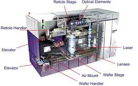
We are used to seeing wafers full of dozens of chips that are then used in processors, but to get there you have to go through a series of steps that start with photolithography .
Transistors are now so incredibly small that manufacturers cannot build them with normal methods. While precision lathes and even 3D printers can make incredibly complex creations, they generally achieve micrometric precision levels (that’s roughly thirty-thousandths of an inch), but they’re still not suitable for the nano-scale scales that machines are made at. chips today.
Photolithography solves this problem by eliminating the need to move complicated machinery with great precision. Instead, it uses light to etch an image onto a silicon chip, as if it were an old overhead projector that could be found in school classrooms but in reverse, reducing the scale of the template to the desired precision.
Thus, the image is projected onto a silicon wafer that is machined with extremely high precision on special machines (the famous machines made by ASML) and under extremely tight conditions, as any speck of dust on the wafer could mean that it will be completely spoiled. The wafer is coated in a material called photoresist, which responds to light and reacts to it, leaving an etching of the CPU that can be filled with copper or other materials to form the transistors. Then, this process is repeated many times increasing the size of the CPU in the same way as a 3D printer accumulates layers of plastic.
The problems with nanoscale photolithography
It doesn’t matter if you can make the transistors smaller and smaller if they can’t work, and nanoscale technology has a lot of problems with physics because of size. Transistors are supposed to stop the flow of electricity when they are off, but they are getting so small that electrons are sometimes able to flow through them. This is called quantum tunneling and it is a huge problem for silicon engineers.
Defects are another problem; even photolithography has a limit in its precision, it is somewhat analogous to a blurry image from the projector, which does not show such a clear image when zoomed in or out. Currently, silicon factories are trying to mitigate this effect by using EUV (extreme ultra violet light) technology, a wavelength much higher than humans can perceive, using lasers in a vacuum chamber. However, this problem will persist as the size continues to shrink.
Sometimes defects can be mitigated with a process called binning: if the defect affects a CPU core, that core is disabled and the chip is sold as a lower-end part. In fact, most CPU lines are made using the same model, but have cores disabled because they have come out defective and are therefore sold at a lower price as a lower-end product.
If the defect hits the cache or other essential component, for example, the chip will likely have to be scrapped, resulting in lower manufacturing performance and therefore higher prices. Current process nodes, such as 7 and even 10 nanometers, have higher throughput rates than 5 nm nodes and therefore the reverse is true, their price is lower.
Packaging, essential in the process of how a CPU is manufactured
Following the process of how a CPU is manufactured, once we have the chips ready, they need to be packaged for consumer use, and this is much more than just putting them in a box with some Styrofoam. When a CPU is finished, it is still useless unless it can be connected to the rest of the system, so the process of “packing” or “packing” refers to the method in which the delicate silicon matrix (the die) is attached to the PCB that most people think of as the CPU.
This process requires a lot of precision, but obviously not as much as the previous steps. The CPU matrix is mounted on a silicon board and the electrical connections run on all the pins that make contact with the motherboard socket. Modern CPUs can have thousands of pins, such as AMD Threadripper processors that have 4096 of them.
Since the CPU produces a lot of heat and must also protect its integrity on the other side, an integrated heat spreader or English IHS is mounted on top. This makes contact with the matrix and transfers heat out of the matrix, which we then cool using a CPU cooler. For some enthusiasts, the thermal paste used to make this connection is not good enough, which makes some decide to do a process of delid to the processor.
Once it’s all set up, it can now be packed into actual boxes, ready to hit store shelves and mount on our computers. Now that you know how a CPU is made and the complexity of making it, it’s a wonder most modern CPUs only cost a few hundred dollars, right?